Dholera Fab Eyes ASML Lithography Equipment
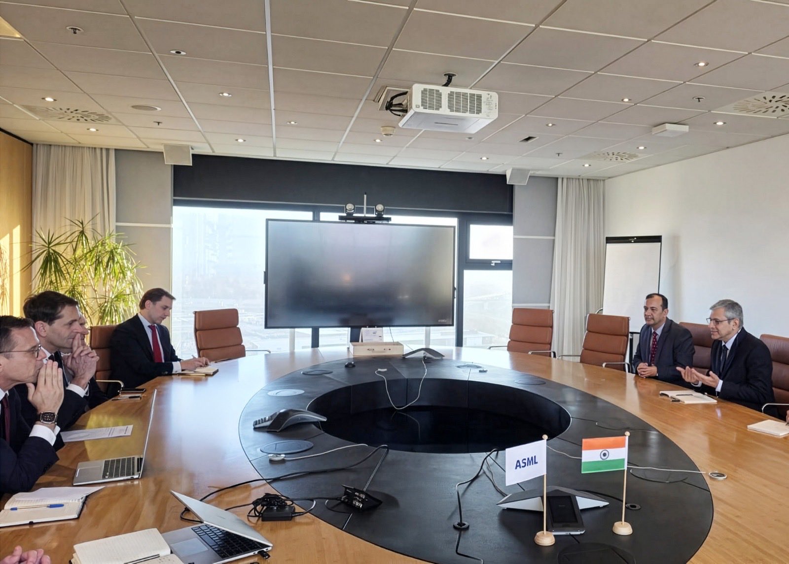
Veldhoven (Netherlands): The semiconductor fabrication facility being developed at Dholera in Gujarat will use lithography equipment supplied by Dutch firm ASML, Union Minister for Electronics and Information Technology Ashwini Vaishnaw said during his visit to the company’s headquarters in the Netherlands, according to an official statement issued on Friday.
Vaishnaw visited the headquarters of Dutch semiconductor equipment manufacturer ASML in Veldhoven today, as part of India’s efforts to strengthen its domestic semiconductor ecosystem, according to an official statement from the Ministry of Electronics and IT.
Speaking during the visit, the minister said India has begun establishing a domestic semiconductor industry and underlined the importance of lithography in chip manufacturing. He described lithography as the most complex and precision-intensive process in the semiconductor value chain, involving the printing of circuit patterns on silicon wafers.
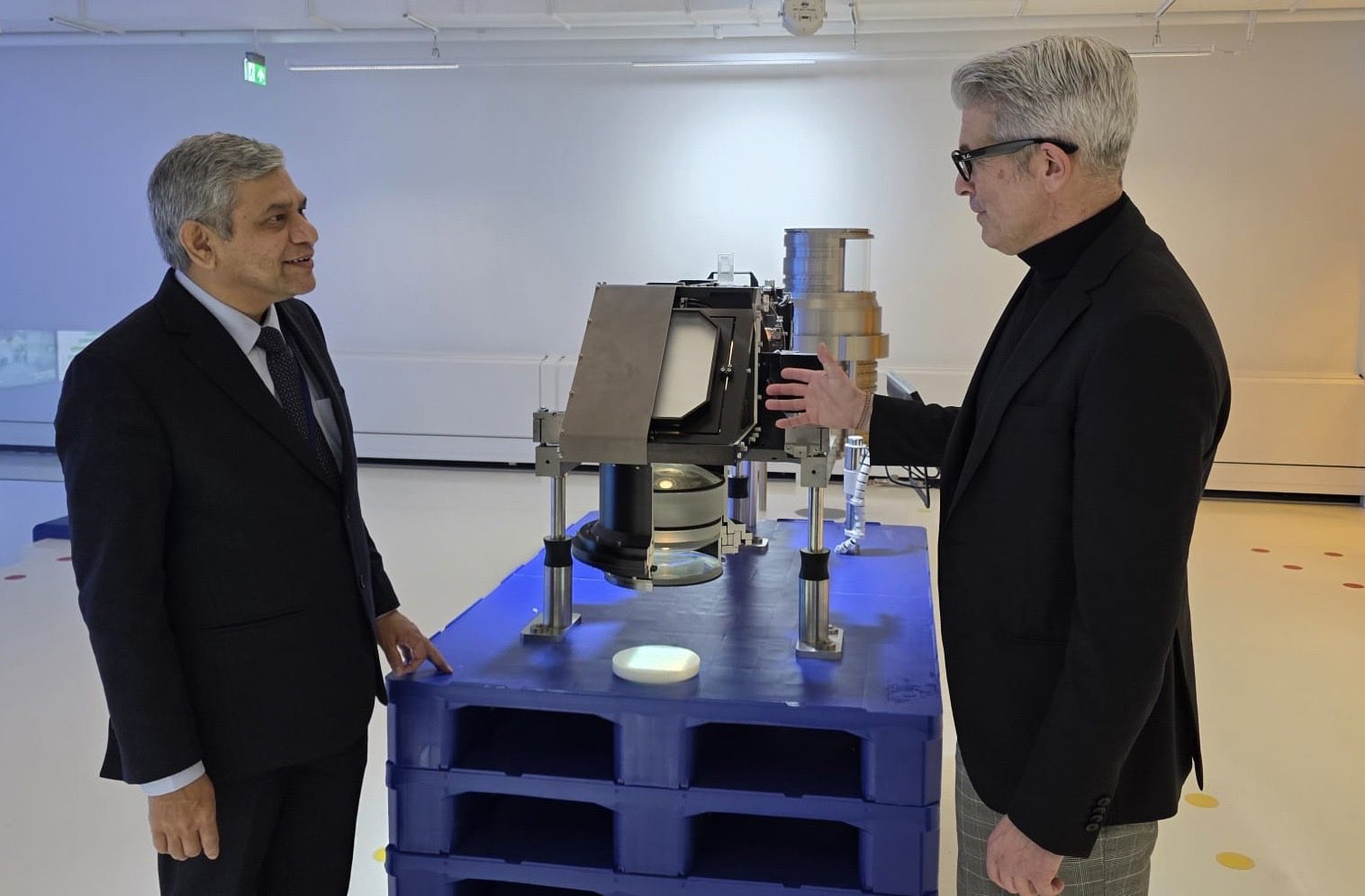
Vaishnaw noted that ASML is the world’s leading provider of lithography tools, enabling the production of nearly every chip manufactured globally. He said that the involvement of ASML in India represents a significant development for the country’s semiconductor ambitions. The minister added that several global equipment manufacturers are exploring opportunities to establish a base in India, citing the country’s design capabilities, large talent pool, and consistent policy framework.
According to the ministry, ASML specialises in the development and manufacture of photolithography machines used to produce integrated circuits. These machines allow chipmakers to mass-produce intricate patterns on silicon wafers, enabling the production of smaller, faster, and more energy-efficient chips. An ASML delegation had participated in SEMICON India 2025, where it expressed interest in partnering with India in its semiconductor manufacturing journey.
The ministry said that the Dholera semiconductor fabrication facility will be among the first in India to deploy ASML’s lithography technology. The project forms a critical part of India’s semiconductor manufacturing strategy and aims to establish a high-tech ecosystem integrating design, fabrication, and assembly. It added that the Dholera fab, equipped with ASML technology, is expected to attract further investment from equipment manufacturers worldwide and strengthen India’s domestic chip design and production ecosystem.
The minister emphasised that India’s skilled workforce, robust policy environment, and growing semiconductor ecosystem are factors drawing global players to establish operations in the country. According to the release, the collaboration is expected to accelerate the production of high-performance, energy-efficient chips for both domestic consumption and export markets.
Vaishnav said India has initiated a domestic semiconductor industry, highlighting the critical role of lithography, the process of printing circuit patterns on silicon wafers, as the most complex and precision-intensive stage in chip manufacturing. “Our fab in Dholera will be using ASML equipment. So I have come here to visit and understand their technology,” he said.
The ministry stated that ASML specialises in photolithography machines used to produce integrated circuits, enabling chipmakers to mass-produce intricate patterns on silicon wafers, resulting in smaller, faster, and more energy-efficient chips. The release added that an ASML delegation participated in SEMICON India 2025, where it expressed a strong interest in becoming a partner in India’s semiconductor journey.
According to the ministry, the Dholera semiconductor fabrication facility in Gujarat will be among the first in India to deploy ASML’s lithography technology. The facility is part of India’s larger semiconductor and electronics manufacturing strategy and aims to establish a high-tech ecosystem integrating design, fabrication, and assembly. The minister emphasised that ASML’s involvement would enhance India’s capabilities in semiconductor manufacturing and support the country’s integration into global chip supply chains.
The ministry expects the Dholera fab, equipped with ASML technology, to attract further investment from equipment manufacturers worldwide and to strengthen India’s domestic chip design and production ecosystem. The minister highlighted that India’s skilled workforce, robust policy environment, and growing semiconductor ecosystem are factors drawing global players to establish operations in the country. According to the release, the collaboration is expected to accelerate the production of high-performance, energy-efficient chips for both domestic consumption and export markets.
– global bihari bureau