Government Advances Student-Led Chip Fabrication Under C2S Programme
122 Student Chip Designs Fabricated at Mohali Lab
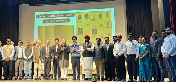
Mohali: Union Minister for Electronics and Information Technology, Ashwini Vaishnaw, handed over 28 chips fabricated at the Semiconductor Laboratory (SCL) here—including 600 bare dies and 600 packaged chips—to students from 17 academic institutions under the Chips to Start-up (C2S) Programme, here on November 28, 2025.
This handover, which took place during the minister’s visit to SCL Mohali and included a review of the ongoing ₹6,700-crore modernisation of the facility and a presentation on the chip design-to-fabrication process, occurs amid broader scrutiny of India’s semiconductor ambitions. This includes delays in attracting foreign investment and achieving sub-100-nanometre node capabilities at public facilities.
SCL Mohali, a key fabrication facility, has packaged and returned the chips to respective institutions, with consolidated design details available on the C2S portal. The programme engages over 200 micro, small, and medium enterprises in the supply chain, though official releases provide no breakdown on per-institution allocations or independent audits of tool usage efficacy.
The chips handed over are real working silicon, but they are made on a 180-nanometre process that is roughly 25 years old—far behind the 3–5 nanometre technology used in today’s smartphones and laptops. The use of a 180-nanometre process node—commercialised globally around 1999—means the chips delivered yesterday remain three to four generations behind current leading-edge nodes (3 nm–5 nm) used in smartphones and high-performance computing, and even lag the 28 nm–40 nm nodes now standard in automotive, 5G, and many defence applications. Power consumption per logic gate is typically 15–30 times higher than at 28 nm, clock speeds rarely exceed 500 MHz, and die area for a given function can be 25–40 times larger, rendering these designs unsuitable for most modern consumer or high-volume commercial products.
The node, however, retains relevance for educational purposes, low-volume IoT sensors, legacy analogue circuits, power-management ICs, and certain long-life-cycle defence systems, but it imposes hard limits on integration density, performance, and energy efficiency. In short, SCL’s 180 nm line serves primarily as a teaching and prototyping platform rather than a commercially competitive foundry.
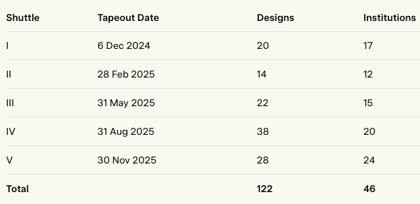
The event underscores efforts to provide industry-grade Electronic Design Automation (Electronic Design Automation; EDA) tools and Multi-project Wafer (Multi-project Wafer; MPW) fabrication services to democratise chip design across Indian universities. The MPW shuttles’ details are as follows:
What matters here is not cutting-edge performance, but the experience. The programme’s tangible achievement is therefore not technological leadership but the exposure of over one lakh students and 1,000 faculty to a complete industry-standard design-to-silicon flow—part of a stated target to train 85,000 engineers under C2S. This hands-on experience is expected to produce graduates familiar with global foundry practices, potentially easing future technology transfer when private-sector fabs at finer nodes eventually materialise. The government hopes this will create a pool of trained engineers ready for the day when proper commercial factories finally open in India.
In the past year, the Chip to Startup (Chip to Startup; C2S) Programme—overseen by the Ministry of Electronics and Information Technology—has facilitated 122 design tapeouts by 46 institutions through five MPW shuttle runs at SCL Mohali, using 180-nanometre technology. Of these, 56 student-designed chips have been successfully fabricated and delivered.
The 122 tapeouts over twelve months, however, represent a fraction of a single day’s output at major international foundries, and the promised upgrade of SCL itself to sub-100 nm nodes remains years away.
The ChipIN Centre, established at the Centre for Development of Advanced Computing (Centre for Development of Advanced Computing; C-DAC) in Bengaluru, aggregates designs every three months, conducts fabrication compliance checks, and combines approved submissions onto single masks to reduce costs and timelines. It supports over 380 organisations with EDA tools, logging more than 175 lakh hours of usage: over 125 lakh hours by more than one lakh students for design, teaching, and research; and about 50 lakh hours by over 90 startups.
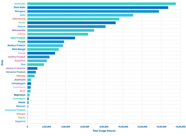
This makes ChipIN Centret one of the world’s largest centralised chip-design user facilities. Following is the State-wise EDA tools usage at various academic institutions.
The following images detail the number of organisations supported with EDA tools in different states of the country:

Vaishnaw described the initiative as creating a “large-scale semiconductor development ecosystem unique to India,” reflecting the government’s vision for self-reliance in strategic sectors through indigenous chips. He emphasised SCL’s pivotal role in building national capabilities to avoid external dependencies, positioning India as a global semiconductor power within years.
– global bihari bureau